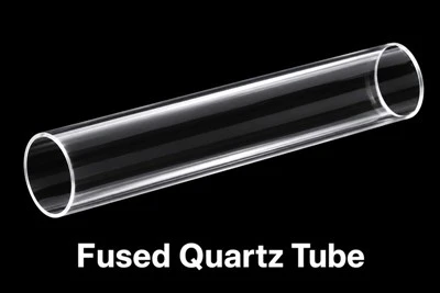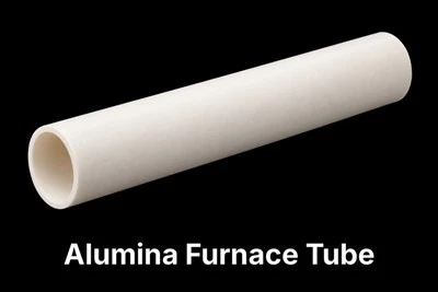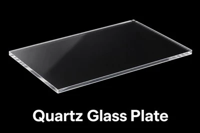
Raw Material Pre-treatment
High-purity quartz sand with a silicon dioxide content of ≥99.99% is selected. It undergoes processes such as acid washing and flotation to keep metal impurities below 5 ppm. The particle size is adjusted to 0.1–0.5 mm to meet subsequent melting requirements.
Main Melting Processes
Vacuum Melting: The material is heated via a temperature gradient of 1650–1800°C, combined with electromagnetic stirring to eliminate melt inhomogeneity; this is the standard melting method in the industry.
Flame Fusion (Gas Melting): An oxy-hydrogen flame serves as the heat source to melt and deposit the raw material into a preform, which is subsequently reheated and drawn into a tube. The resulting product features low bubble content and high purity, making it ideal for optical fiber manufacturing.
Synthetic Melting: Methods such as CVD and PCVD use high-purity silicon-containing compounds as raw materials, processed via high-temperature oxidative deposition. This achieves extremely low hydroxyl content, suitable for high-end semiconductor and optical applications.
Forming and Post-processing
VAD (Vapor-phase Axial Deposition) or CNC tube-drawing processes are employed to control wall thickness tolerance within ±0.1 mm; high-precision drawing machines can achieve a diameter control accuracy of ±0.05 mm.
The tubes undergo a stepped, slow-cooling process from 800°C to room temperature at a rate of 15°C/h to completely eliminate internal stress, preventing cracking or deformation during subsequent use.
Finished products are obtained after completing comprehensive quality verification, including ultrasonic cleaning and precision inspection.